ENIG 2.0mm Multi-layers 1oz HDI PCB Printed Circuit Board
HDI PCB Board Introduction
High Density Interconnection,shorted as (HDI) PCB, is a kind of (technology) for the production of printed circuit boards. It is a circuit board with relatively high circuit distribution density using micro blind via and buried via technology. Adopting the structure of Stripline and Microstrip, multi-layering becomes a necessary design. In order to reduce the quality problem of signal transmission, insulating materials with low dielectric constant and low attenuation rate are used. To meet the miniaturization and arraying of electronic components, the density of circuit boards is constantly increasing to meet the demand.
PCB CAPABILITIES
| FACTORY CAPABILITIES |
| No. | Items | 2019 | 2020 |
| 1 | HDI Capabilities | HDI ELIC (4+2+4) | HDI ELIC(5+2+5) |
| 2 | Max layer count | 32L | 36L |
| 3 | Board Thickness | Core thickness 0.05mm-1.5mm ,Fineshed board thickness 0.3-3.5mm | Core thickness 0.05mm-1.5mm ,Fineshed board thickness 0.3-3.5mm |
| 4 | Min.Hole Size | Laser 0.075mm | Laser 0.05mm |
| Mechnical 0.15mm | Mechnical 0.15mm |
| 5 | Min Line Width/Space | 0.035mm/0.035mm | 0.030mm/0.030mm |
| 6 | Copper Thickness | 1/3oz-4oz | 1/3oz-6oz |
| 7 | Size Max Panel size | 700x610mm | 700x610mm |
| 8 | Registration Accuracy | +/-0.05mm | +/-0.05mm |
| 9 | Routing Accuracy | +/-0.075mm | +/-0.05mm |
| 10 | Min.BGA PAD | 0.15mm | 0.125mm |
| 11 | Max Aspect Ratio | 10:1 | 10:1 |
| 12 | Bow and Twist | 0.50% | 0.50% |
| 13 | Impedance Control Tolerance | +/-8% | +/-5% |
| 14 | Daily Output | 3,000m2 (Max capacity of equipment) | 4,000m2 (Max capacity of equipment) |
| 15 | Surface Finishing | ENEPING /ENIG /HASL /FINGER GOLD/IMMERSION TIN/SELECTIVE THICK GOLD |
| 16 | Raw Material | FR-4/Normal Tg/High Tg/Low Dk/HF FR4/PTEE/PI |
The types of HDI PCB
1.through vias from surface to surface,
2.with buried vias and through vias,
3.two or more HDI layer with through vias,
4.passive substrate with no electrical connection,
5.coreless construction using layer pairs
6.alternate constructions of coreless constructions using layer pairs.
HDI (High Density Interconnection) circuit boards usually include laser blind vias and mechanical blind vias; general through buried vias, blind vias, stacked vias, staggered vias, cross blind buried, through vias, blind via filling plating, fine line small gaps, The technology of realizing the conduction between the inner and outer layers by processes such as micro-holes in the disk, usually the diameter of the blind buried is not more than 6 mils.
Work flow for HDI
Board Cut - Inner Wet film -DES - AOI - Brown Oxido - Outer Layer Press - Out Layer Lamination - X-RAY & Rounting - Copper reduce & brown oxide - Laser Drilling - Drilling - Desmear PTH - Panel plating - Outer Layer dry film - Etching - AOI- Impedance Testing - S/M Pluged hole - Solder Mask - Component Mark - Impedance testing - Immersion Gold -V-cut - Routing - Electrical Test - FQC - FQA -Package -Shipment
Similar products
HDI PCB Board Application Field
Our PCB are widely used in communication equipment, industrial control, consumer electronics, medical equipment, aerospace, light-emitting diode lighting, automotive electronics etc.
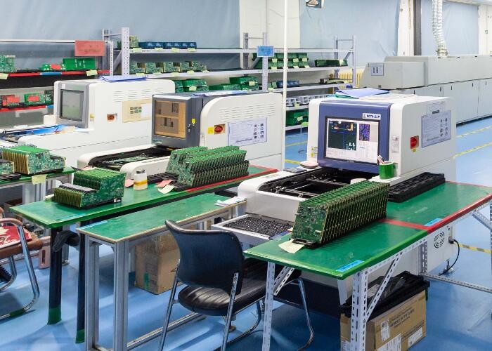
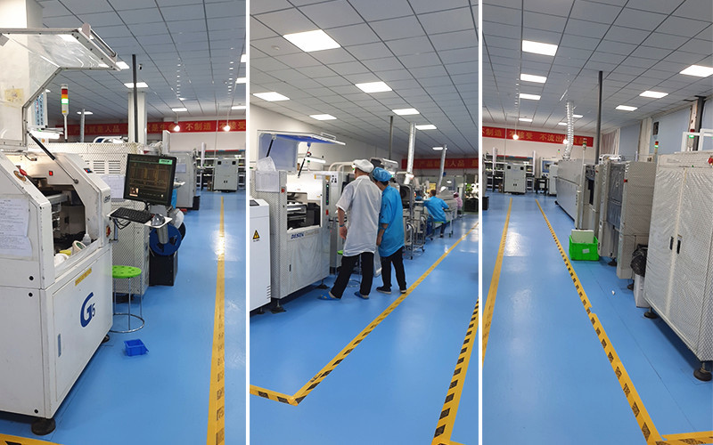
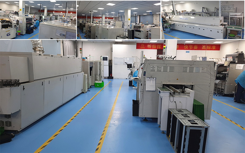
Workshop
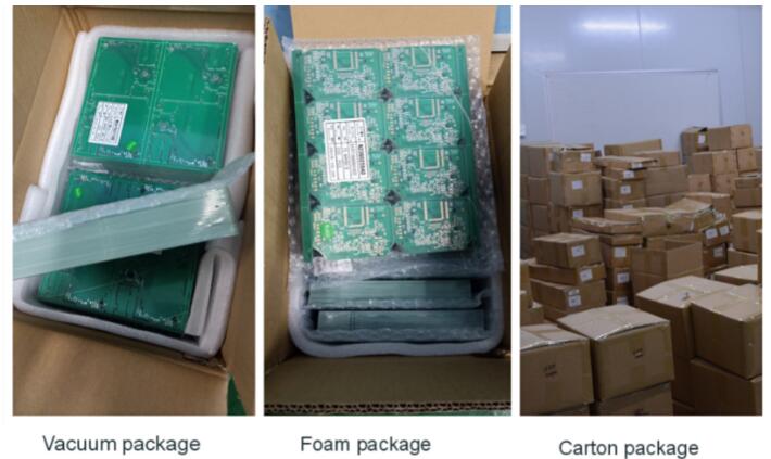
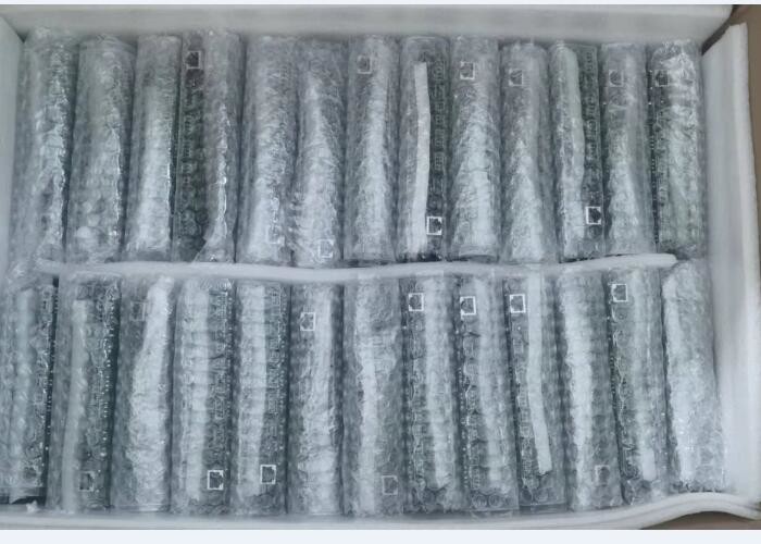
Common packaging
1.PCB: Vacuum packaging with carton box
2.PCBA: ESD packaging with carton box
Our advantage
1.Service value
Independent quotation system to quickly serve the market
2.PCB manufacturing
High-tech PCB and PCB assembly production line
3.Material purchasing
A team of experienced electronic component procurement engineers
4.SMT post soldering
Dust-free workshop, high-end SMT patch processing
FAQ
Q1:What kind of PCB file format can you accept for production?
Gerber, PROTEL 99SE, PROTEL DXP, CAM350, ODB+(.TGZ)
Q2:Is my PCB files safe when I submit them to you for manufacturing?
We respect customer's copyright and will never manufacture PCB for someone else with your files unless we receive written permission from you, nor we'll share these files with any other 3rd parties.
Q3:What payments do you accept ?
-Telex Transfer(T/T),Western Union,Letter of Credit(L/C)
-Paypal,AliPay,Credit Card
Q4:How to get the PCB?
A:For small packages, we will ship the boards to you by DHL,UPS,FedEx,EMS. Door to door service! You will get your PCBs at your home.
B:For heavy goods more than 300kg, we may ship your boards by ship or by air to save freight cost. Of course, if you have your own forwarder, we may contact them for dealing with your shipment.
Q5:What is your minimum order quantity?
Our MOQ is 1 PCS.
Q6: Can we visit your company?
No problem. You are welcome to visit us in Beijing. Or the branch factory is in Tianjin.
Q7: How can you ensure the quality of the PCB?
Our PCBs are 100% test including Flying Probe Test, E-test and AOI.
Product Tags:

|
|
Through Vias ENIG 2.0mm Hdi Pcb Board 8layers 1oz Images
|


